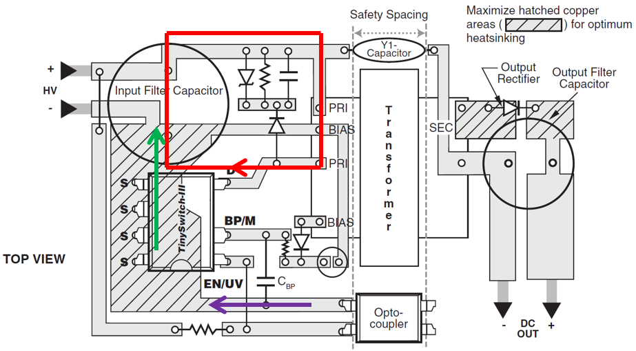
Three check points
- Switch loop: Try to find the power device
- MOSFET
- Diode
- Reduce the switch loop circle area in the layout; Keep switching loops as small as possible
- Can’t put any signal components inside or around the switch loop
- Power and signal loop: Try to find the power path
- MOSFET
- Diode
- Mostly is related with switch loop ,B+ and B-; Kelvin connection
- Power path is needed to be separated with signal path; Switching loops need totally separated with signal loops
- Small Signal components as close as possible the device’s pin
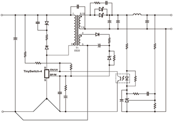
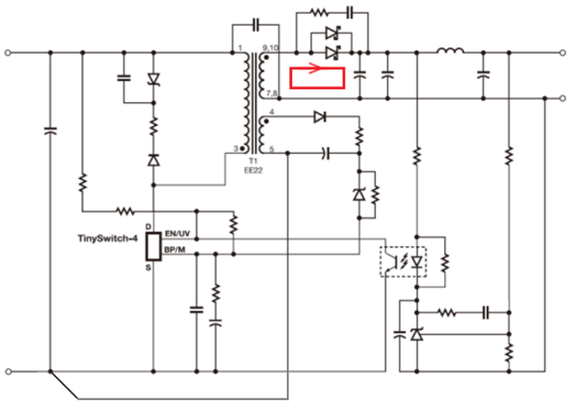
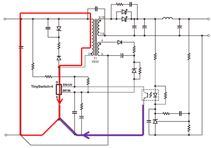
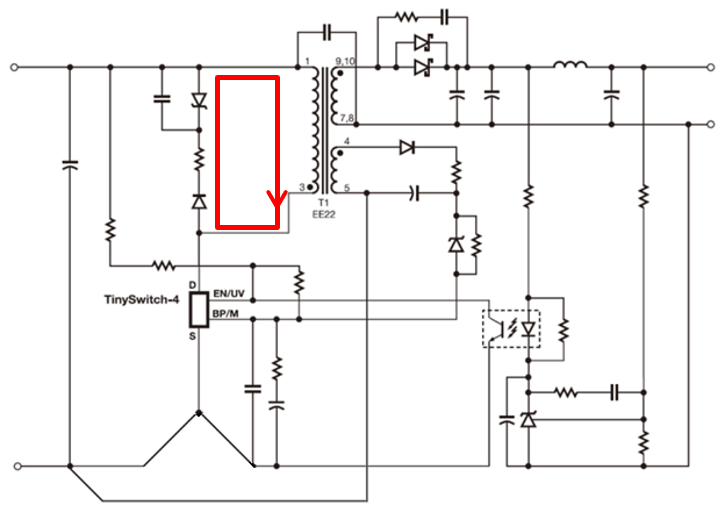
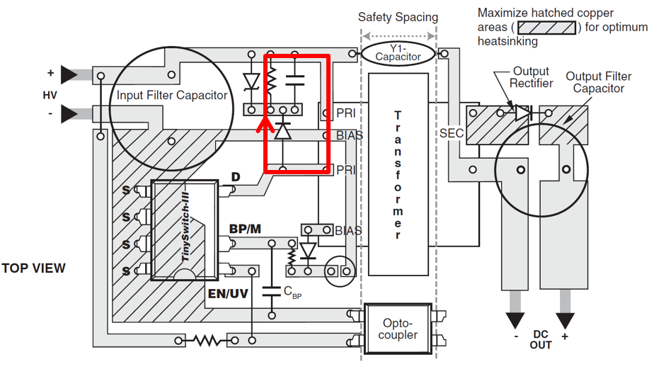
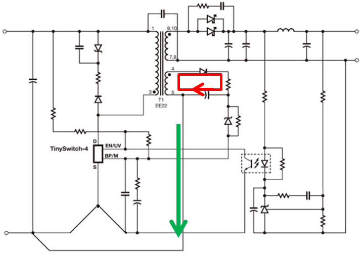
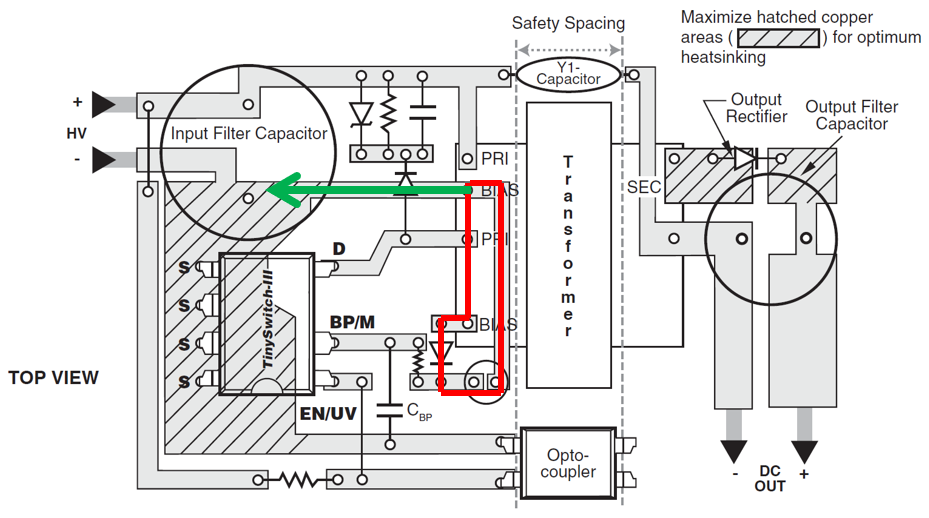
Switch loop of Standard schematic for Tiny switch
Normal we will separate to 4 switch loops in a standard circuit
- Snubber should be noted too
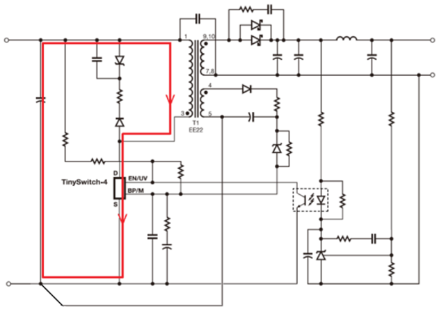
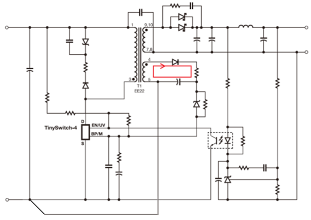
1.Main Mosfet switch loop
- The Green line, MOSFET currents flow into Bulk cap directly; the Signal loops need to pass through Source pin, can’t connect with high current path between Source pin to Bulk cap(Green line)
- The purple line, it’s the Signal ground. High current will flow in Bulk cap(Green line), purple path has no switch current
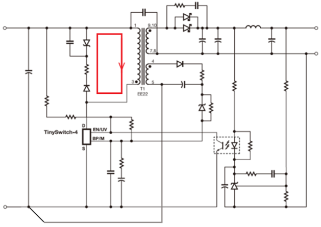
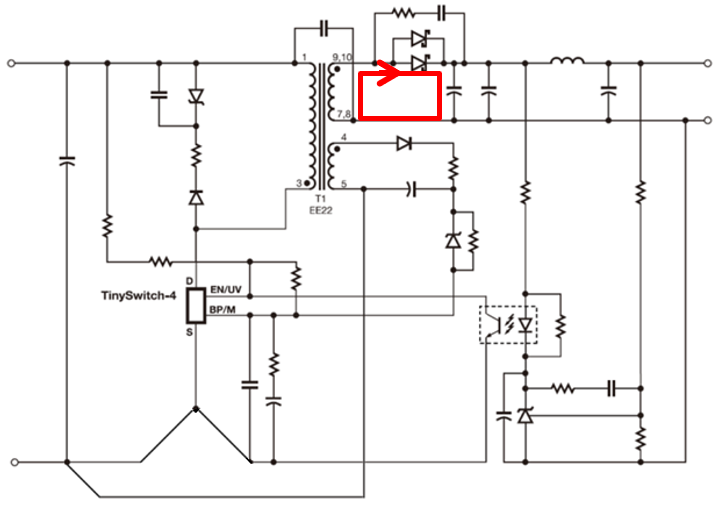
2. Primary snubber loop
- B+ of Main transformer → Clamp diode → TVS or RC → B+
3. Primary bias winding loop
- Bias winding high side → Rectifier Diode → Capacitor → Bias winding low side
- The Green line, bias winding currents flow into Bulk cap directly; the Aux Ground need totally separated with signal loops and don’t pass through Tny’s Source pins when it back to Bulk cap Ground
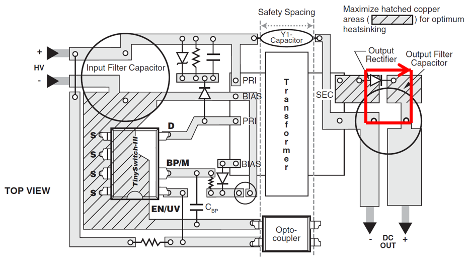
4. Secondary power winding loop
- Output winding high side → Rectifier Diode → Capacitor → Output winding low side
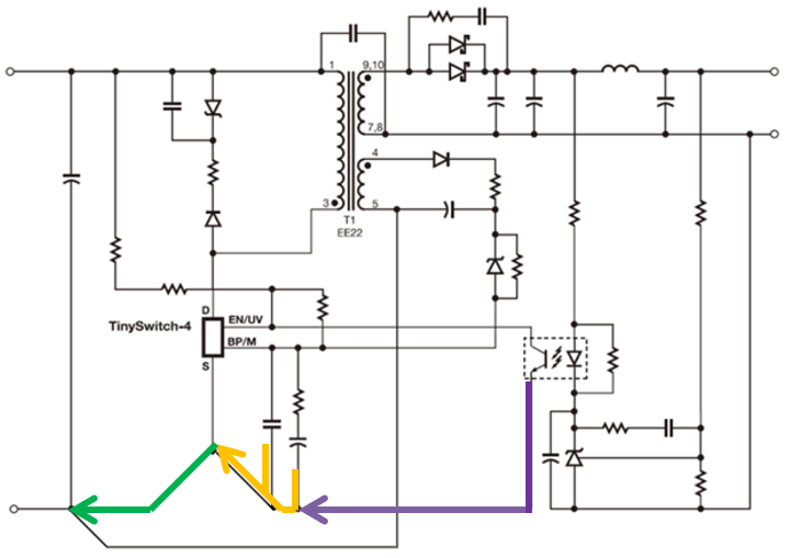
5. Signal loop
- Yellow & purple line is clean ground. Signal components connect to source pin directly without through power path (Green line is non-clean; power current flow into bulk cap)
- Signal components and trace can’t be closed switch loop, especially Drain pin (trace) or snubber circuit (Because high dv/dt)

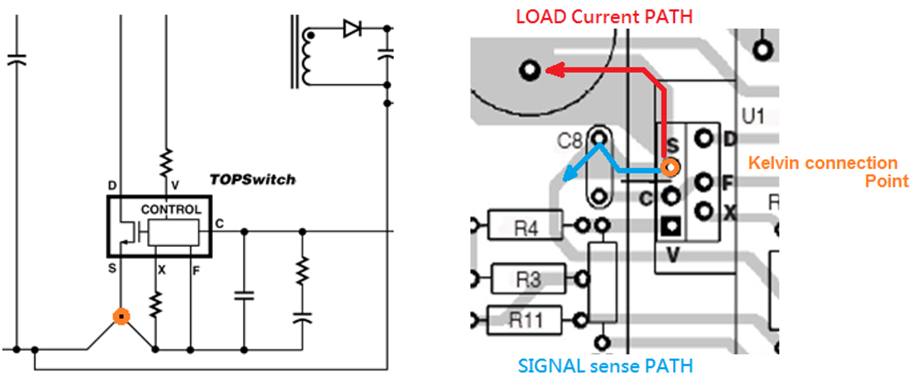
What's Kelvin connection?
A Kelvin connection is a means of making precision electrical potential contact with a current carrying component or reference point in such a way that eliminates or greatly reduces the effect of contact resistance.