(Latching shutdown triggers when BP/M pin current > 6 mA for >30 μs)
BYPASS/MULTI-FUNCTION (BP/M) Pin provides a shutdown function. When the current into the bypass pin exceeds ISD, the device latches off until the BP/M voltage drops below 4.9 V, during a power-down or, when the UV function is employed with external resistors connected to the BP/UV pin, by taking the UV/EN pin current below IUV minus the reset hysteresis (Typ. 18.75 μA). This can be used to provide an output overvoltage function with a Zener connected from the BYPASS/MULTI-FUNCTIONAL pin to a bias winding supply.

Latching Shutdown OVP
(The most Accurate OVP from secondary side)
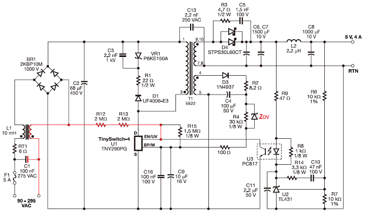
In OVP testing, the output voltage will be increased and Increase Zener's Reverse voltage to over than Zener(ZOV) breakdown. Zener breakdown occurs and NPN bipolar junction transistor will short Collector and Emitter(Ground) immediately.
The opto-coupler (UOV) go through current, transfer an electrical signal to primary side and current begins to flow into the BYPASS/MULTI-FUNCTIONAL pin. When this current exceeds ISD the internal latching shutdown circuit in TinySwitch-4 is activated.
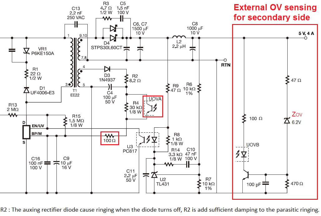
Accurate OVP from secondary side
In OVP testing, the output voltage will be increased . When reverse biased voltage applied to the Zener diode reaches Zener breakdown (ZOV), it starts allowing large amount of electric current. This current will go through opto-coupler (UOV) . This current will be impacted by output voltage.
The opto-coupler (UOV) go through this current , transfer an electrical signal to primary side and current begins to flow into the BYPASS/MULTI-FUNCTIONAL pin. When this current exceeds ISD the internal latching shutdown circuit in TinySwitch-4 is activated. Base on Zener breakdown characteristic, this current is also impacted by output voltage. Normally, OVP voltage will be higher than last page solution.
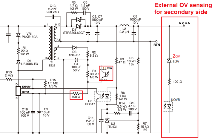
Simple OVP from Primary side
(simple, low cost, primary side design)
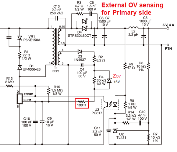
In OVP testing, the output voltage will be increased and the aux winding will also be increased. When aux winding voltage applied to the Zener diode reaches Zener breakdown (ZOV), it starts allowing large amount of electric current. This current begins to flow into the BYPASS/MULTI-FUNCTIONAL pin. When this current exceeds ISD the internal latching shutdown circuit in TinySwitch-4 is activated.
Filtering resistor (R2 = 10 - 47 Ω) can be added to minimize the error voltage on the bias winding due to leakage inductance
The other method is replaced the D3 and R2 to a single standard diode (slower) to minimize the error voltage on the bias winding
Higher bias winding voltage (15- 30 V) is recommended for more precise OVP threshold.
Base on Zener breakdown characteristic, this current is also impacted by aux winding voltage. But the aux winding voltage will be different with different output loading. So the OVP can’t be accurate in this circuit ,but it’s simple.
Auto Restart OVP
From Secondary side
BYPASS Pin only can provides a shutdown function. We need more different circuity to achieve auto restart symptom.
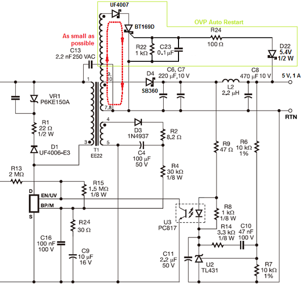
Put a stack winding and SCR circuity as Green circle.
The SCR sink current from stack winding while OVP sensing Zener diode (D22) breakdown.
The winding turns should be more enough to avoid to damage the SCR.
The SCR placement should be as close as transformer winding in the layout.
Auto Restart OVP
From Primary side (only for Tiny Switch 4)
As we said before, one condition can reset BP latch off function when the UV/EN pin current below IUV minus the reset hysteresis (Typ. 18.75 μA).
EN/UV pin external resistors connected to the AC line or nature, current flowing through R12 and R13 drop below 18.75 μA each AC line half-cycle ,therefore non-latching for an overvoltage fault.
Latching over-voltage protection can be achieved by connecting R12 and R13 to the positive terminal of C2, at the expense of higher standby consumption. In the example shown, on opening the loop, the OVP trips at an output of 17 V.
This circuity has some impact as followed,


