|
innoSwitch 3 Layout Note |
|
| 2021年6月8日 | |
|
Recommendations for Circuit Board Layout
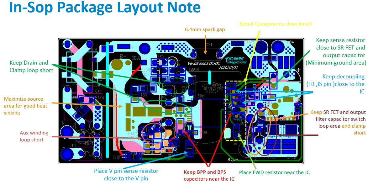
Single-Point Grounding - Use a single-point ground connection from the input filter capacitor to the area of copper connected to the SOURCE pin. Bypass Capacitors - The PRIMARY BYPASS (CBPP), SECONDARY BYPASS (CBPS) decoupling capacitors must be located directly adjacent to the PRIMARY BYPASS-SOURCE, SECONDARY BYPASS-GROUND and FEEDBACKGROUND(CFB) pins respectively and connections should be routed via short traces. Signal Components - External components RLS, RBP, RFBv(UPPER), RFB(LOWER) and RIS which are used for monitoring feedback information must be placed as close as possible to the IC pin with short traces. Critical Loop Area - Circuits where high dv/dt or di/dt occurs should be kept as small as possible. The area of the primary loop that connects the input filter capacitor, transformer primary and IC should be kept as small as possible. - No loop area should be placed inside another loop. - included Primary and secondary switching and Clamp Circuit Y Capacitor - The placement of the Y capacitor should be directly from the primary input filter capacitor positive terminal to the output positive or return terminal of the transformer secondary. Such a placement will route high magnitude common mode surge currents away from the IC. ESD Immunity - Sufficient clearance should be maintained (>8 mm) between the primary-side and secondary-side circuits to enable easy compliance with any ESD or hi-pot isolation requirements. Drain Node - The drain switching node is the dominant noise generator. As such the components connected the drain node should be placed close to the IC and away from sensitive feedback circuits. 
This's a roughly layout note for innoSwitch 3 family |
|
|

