- Soft turn-off
在所謂的智能驅動IC,因為是智能,所以都會提供更多的功能,像是短路保護機制,一般會透過偵測 IGBT 在短路發生時,進入退飽和的行為來作為短路發生的判斷。
而在偵測到短路發生後透過關斷行為,來對系統做保護。
由於迴路中雜散電感的存在,在短路發生時產生的電流相當大,如果你直接去關閉這大電流,會因為關閉的這大 di/dt 在迴路上產生極大電壓尖波。這尖波造成 IGBT 的過壓而損壞。
為了讓關閉時的 di /dt 降低,改變 IGBT 關閉的速度,變成了一個很有效的策略。
所有廠家所採用的策略大致相同,不過當然在細部操作上還是有些差異,因而衍生了各家自行定義名稱也多少有些差異。
不過不用太在意,其實觀念都是類似的,目的也是一樣的。
The soft turn-off was reducing the turn-off overvoltage even more than expected
Due to the presence of the parasitic inductance in the loop, turning the power switch off too quickly under a high fault current condition can generate a high voltage spike at the power switch collector.
The IC activates additionally a soft turn-off sequence, if a turn-off is initiated due to a desaturation condition on terminal DESAT.
Common Description
- shutdown
- turn-off
- s“softly” turn-off
IGBT is shut off slowly
Infineon
- two-level turn-off
- Zener diode controls the level, & TLSET pin set timing
TI
- Three discharged timings
- Zener diode controls the level, & resistor set timing Silicon Labs
- Two discharged timings
- Internal resistor set timing & External Resistor can increase discharged time
Avago
- Two discharged timings
- Internal MOSFET’s Rds(on) resistor set timing
- One discharged timing
- External Soft Shutdown Resistor set timing
PI
- Two discharged timings
- Time constant
- One discharged timing
- Time constant
Infineon (EiceDRIVERTM)
The IGBT can be turned off smoothly via an external higher-ohmic gate resistor attached to terminal SOFF. The soft turn-off speed can be adjusted by selecting the appropriate resistor value. The soft turn-off reduces the voltage overshoot considerably and may be used in combination with the two-level turn-off function of the IC.
Two-Level Turn-Off (1ED020I12BT only)
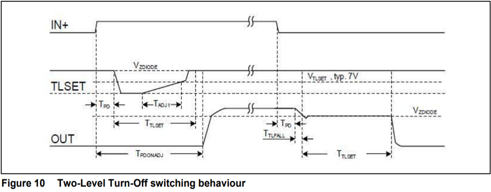
The Two-Level Turn-Off introduces an additional turn off voltage level VZDIODE (as shown in Figure 10) at the driver output in between ON- and OFF-level. This additional level ensures lower VCE overshoots at turn off by reducing gate emitter voltage of the IGBT in short circuits. The lowered VGE level is limiting the current of the IGBT during the additional level interval TTLSET, the required timing value is depending on stray inductance and di/dt at beginning of two level turn off interval.
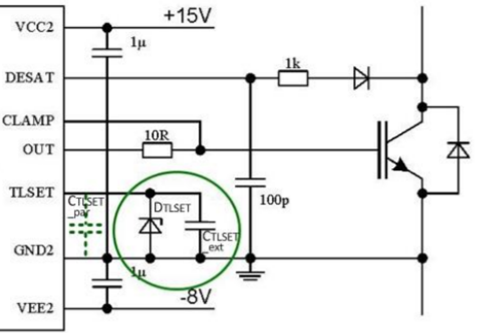
The additional turn off voltage level VZDIODE and hold up time TTLSET could be adjusted at TLSET pin. The VZDIODE is set by the external Zener diode DTLSET connected between pin TLSET and GND2. The interval TTLSET is set by the external capacitor CTLSET_ext connected to the same pin TLSET and GND2.
Texas Instruments
The VCE of the IGBT is monitored during ON time to detect overcurrent conditions, which will make the IGBT get into a linear mode of operation. On detecting VCE higher than a DESAT threshold, the IGBT is shut off slowly (soft turnoff) to limit the VCE overshoot.
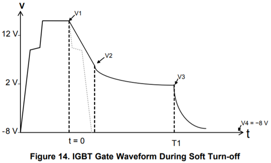
A soft turn-off is done by increasing the gate voltage discharge time during turn-off to reduce the di/dt after a DESAT fault condition
Two functions
- One is to discharge the gate capacitance until it reaches 2 V and then to strongly apply –8 V to the gate to keep the IGBT turned off.
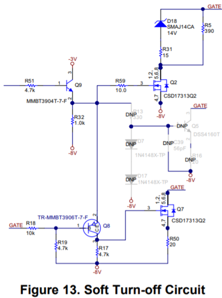
After the DESAT-DETECT signal goes high, Q9 turns-on and causes Q2 to turn on, which engages the Zener and resistor to discharge the gate. Once the gate voltage reduces to 2 V, the clamp circuit (Q8 and Q7) is activated. Q8 is used as a comparator by comparing the gate voltage with the base emitter saturation voltage (VBE_sat) of 0.85 V.
Design Processes Flexible High Current IGBT Gate Driver With Reinforced Digital Isolator
Silicon Labs
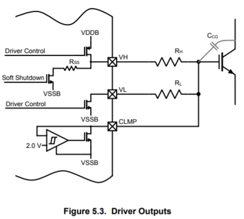
To avoid the high turn-off voltage spike, only the soft shutdown NMOS is turned on under DSAT shutdown (while the VL NMOS is kept in the off state). The gate capacitance of the power switch is discharged through the RH and the internal Rss at a much lower rate to allow the power switch to dissipate residual energy.
(AN1009)
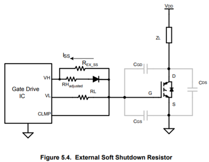
The internal Rss (30 Ω) and a RH = 20 Ω provide a typical soft shutdown duration of 2 μs (for 250 nC of total gate charge, Qg.) If a longer soft shutdown period is required, steering diode (ES1B or similar) can be added to the VH pin to allow installation of a larger external soft shutdown resistor (see figure below).
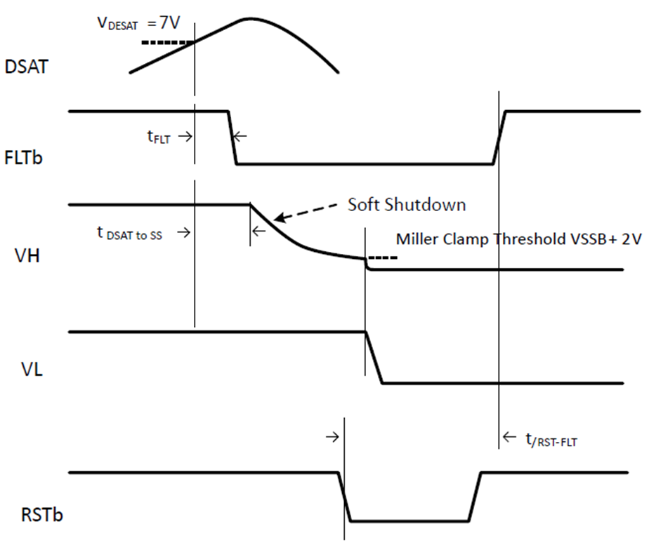
If the voltage on the DSAT pin exceeds 7 V during on-time, the Si828x shuts down the output (turn off VH PMOS after tFLT delay) and initiates soft shutdown (after tDSAT to SS delay) to protect the power switch.
Avago
A “soft” shutdown sequence, reducing the IGBT current to zero in a controlled manner to avoid potential IGBT damage from inductive over voltages.
When a DESAT fault is detected, VOUT(VGE) is slowly brought low in order to “softly” turn-off the IGBT and prevent large di / dt induced voltages
Avago (AN5315) When a desaturation fault is detected, a weak pull-down device in the ACPL-332J output drive stage will turn on to ‘softly’ turn off the IGBT. This device slowly discharges the IGBT gate to prevent fast changes in drain current that could cause damaging voltage spikes due to lead and wire inductance. During the slow turn off , the large output pull-down device remains off until the output voltage falls below VEE + 2 Volts, at which time the large pull down device clamps the IGBT gate to VEE.
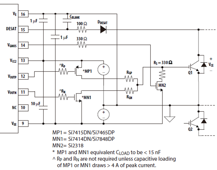
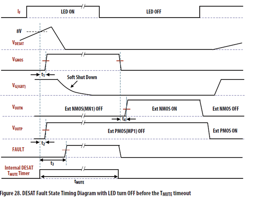
Avago (ACPL-339J) When a DESAT fault is detected, VGMOS switches from low to high, turning on an external MN2 pull down switcher. MN2 slowly discharges the IGBT gate at a decay rate corresponding to the RC constant of RS and CIN (IGBT input capacitance).
PI (SSD Soft Shut Down)
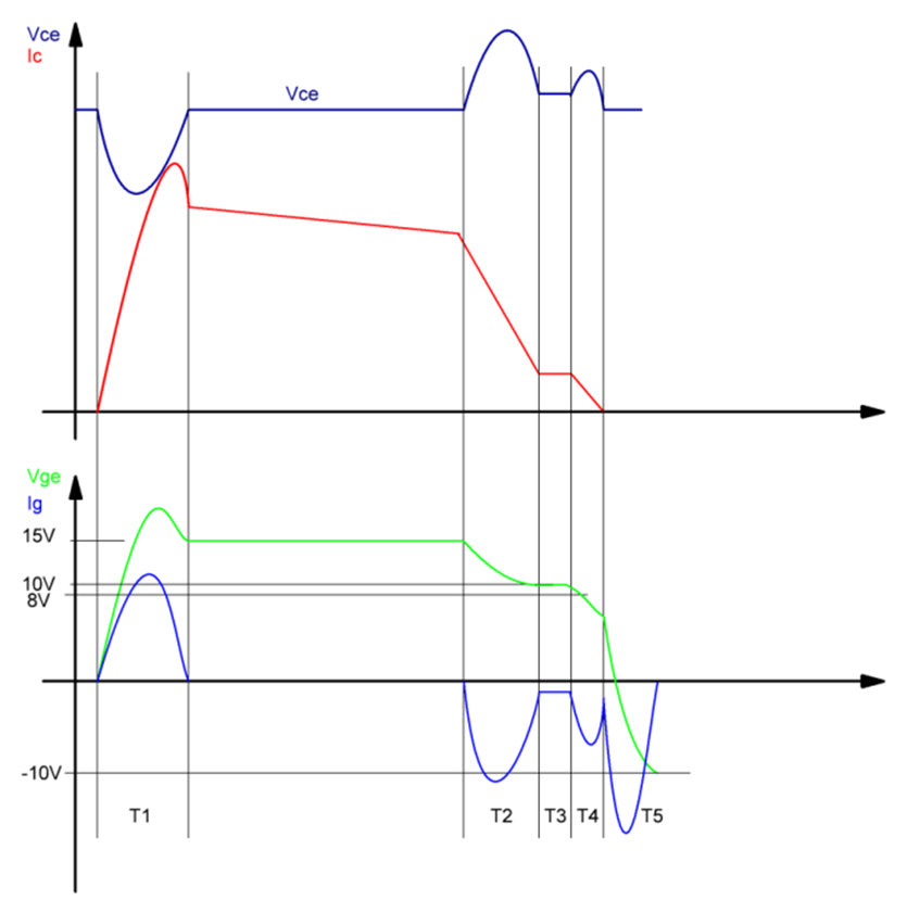
T1 → IGBT desaturates
T1 - T2 → short circuit detection
T2 → gate-emitter voltage decreases from 15V to approx 10V in defined time of 2μs
T3 → gate emitter voltage is stabiles on approx 10V, ScaleTM - 2 measures gate current
T4 → at end of T3 the gate current was nearly zero, gate – emitter voltage decreases with defined speed to approx. 5V
T5 → ScaleTM - 2 applies negative voltage
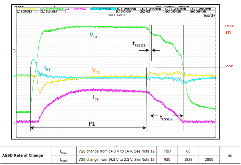
ASSD – Advance Soft Shut Down
Key parameters:
- tFSSD1 – first decrease in VGE
- tFSSD2 – first decrease in VGE
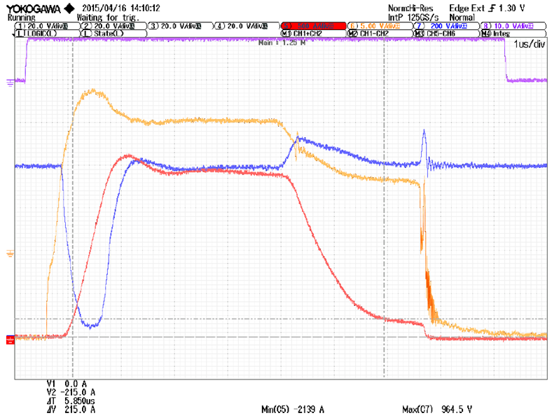
Those two timings combined with voltage levels are responsible for temporary VCE overvoltage.
逐步監測及降驅動電壓的軟關斷技術
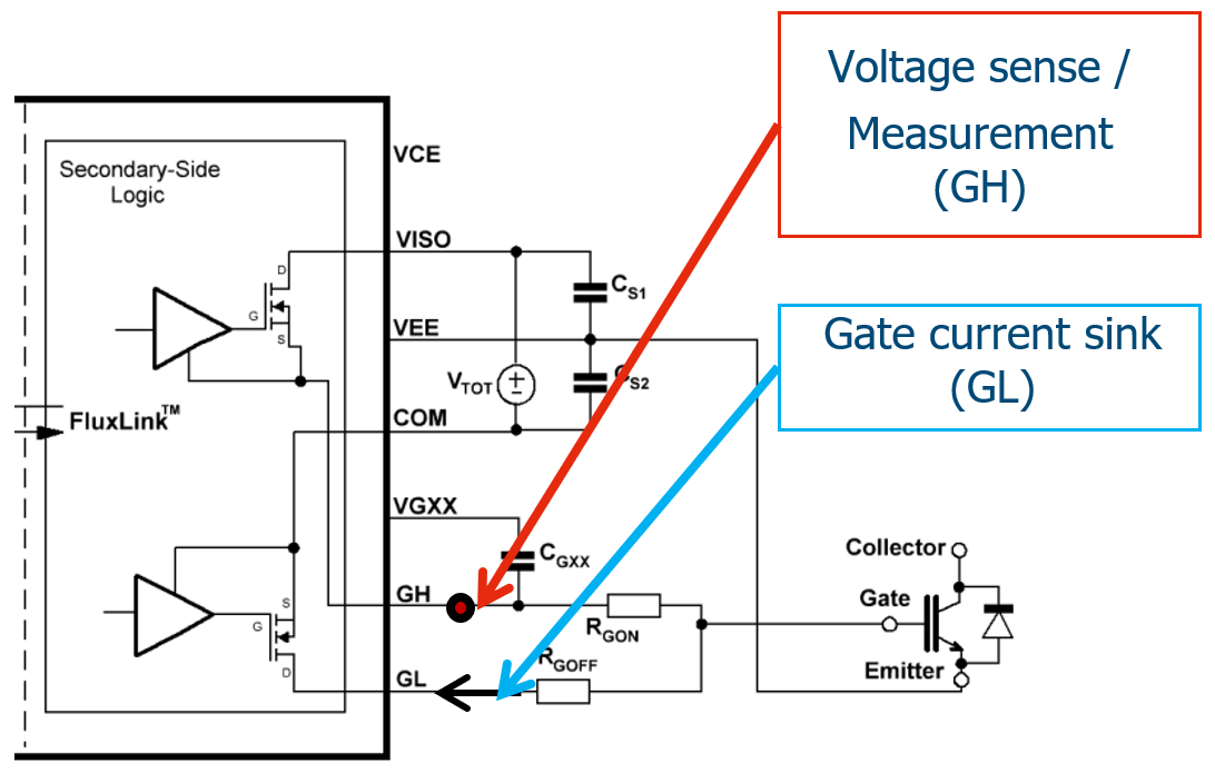
ASSD功能用 GH 腳檢測 Gate 電位,用 GL 腳對柵極進行放電;
全過程的時間被 Scale iDriver 控制住
